Page 36 - libroBrevetti
P. 36
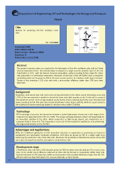
Department of Engineering, ICT and Technologies for Energy and Transport Patent Title Method for producing thin-Įlm mulƟlayer solar cells. Ref. CNR 10000 Assignee(s): CNR CNR InsƟƚute: IMEM Main Inventor: Edmondo Gilioli Countries: IT Priority date: 21/11/2008 Abstract The present inveŶƟŽn refers to a method for the ĨĂďƌŝĐĂƟon of thin Įůŵ ŵƵůƟlayer solar cells by Pulsed Electron DeposŝƟŽn (PED). This method allows to deposit in a single step the absorber layer of the ceůů͕ Cu(InGa)Se2 or CIGS͕ with the desired chemical composŝƟŽŶ͕ without needing further stages for ĐĂƟŽn rĂƟŽ adjustment or seleŶŝnjĂƟŽn treatments. Moreover all the layer of the cell ;ďƵīer layer͕ transparent ĐŽŶĚƵĐƟng oxide) can be grown by PED in the same vacuum system͕ by rotaƟng a mulƟ-target carrousel. Thanks to this technique͕ CIGS solar cells with a photovoltaic ĞĸĐŝĞŶĐy larger than 17% have been fabricated. Background EŽǁĂĚĂLJƐ͕ /'^ͲďĂƐĞĚ ƐŽůĂƌ ĐĞůůƐ ƌĞƉƌĞƐĞŶƚ Ă ƐƚƌŽŶŐ ĂůƚĞƌŶĂƟǀĞ ƚŽ ƚŚĞ ƐŝůŝĐŽŶͲďĂƐĞĚ ƚĞĐŚŶŽůŽŐLJ͕ ƐŝŶĐĞ ŽŶůLJ 1/100 of the raw materials is needed to absorb the same solar light quanƟty as the Si cells and to convert it into electrical current. Such a huge material saving mainly means reduced electricity costs: the electrical power produced by thin-Įlm solar cells already raised lower values than 0.50$/Wp͕ while the costs related to the trĂĚŝƟŽŶĂl Si-based technology hinders to decrease them under 0.70$/Wp. Technology PED technology is based on the interĂĐƟŽn between a pulsed high-power e-beam and a bulk target of the material to be deposited as thin film (i.e. CIGS). The energy exchange between e-beam and target leads to an immediate abůĂƟŽn of the ůĂƩĞƌ͕ which evaporates as high-energy plasma and condensates on a substrate faced in front of it. This evaporĂƟŽn occurs out of thermodynamic equilibriuŵ͕ thus preserving the target stoichiometry on the thin Įům. Advantages and ApplicaƟons While the tradiƟonal approaches to CIGS deposŝƟŽn (thermal co-evaporĂƟŽn or sƉƵƩering) are based on complicated and subsequent mulƟ-step treatments͕ CIGS Įlms are grown by PED in a single stage͕ thus enhancing the ƉƌŽĚƵĐƟŽn rate of the solar cells. Moreover the possibility to fabricate the whole cell by PED can reduce the deadͲƟŵĞ and the atmospheric conƚĂŵŝŶĂƟŽn risks. Development stage 17%-Ğĸcient solar cells with a CIGS absorber grown by PED have been recently obtained. This result is very close to the world record Ğĸciency achieved on CIGS cells by thermal co-evapŽƌĂƟŽn (20%). Solar cells enƟrely fabricated by PED (absorber͕ ďƵīer and transparent oxides) exhibit eĸciencies larger than 6%. 5%- eĸĐŝent cells have been fabricated onto unusual substrates͕ as Ɵůe or plasƟĐ͘ 27